10+ pwm block diagram
The microcontroller unit provides 8-bit input into PWM module. The high frequency PWM AC signal.

Ch 10 Pulse Width Modulation Education And Teaching Arduino Forum
Working principle of the generator is simple.

. As weve seen in the previous tutorial STM32 PWM As A DAC the PWM peripheral in STM32 microcontrollers can be used as a DAC to output analog voltage that corresponds to the duty cycle of the PWM signalHence generating analog waveforms is nothing more than writing out the waveform data points from somewhere in the. 16-channel 12-bit PWM Fm I2C-bus LED controller 5. 8 gpio 14 uart tx 10 gpio 15 uart rx 12 gpio 18 pcm clk 14 ground.
A duty cycle and a frequency. 15 Block Diagram 5 2 Pin Definitions 6 21 Pin Layout 6 22 Pin Description 6 23 Power Scheme 8 24 Strapping Pins 9 3 Functional Description 10 31 CPU and Memory 10 311 CPU 10 312 Internal Memory 10 313 External Flash and SRAM 10 314 Memory Map 11 32 Timers and Watchdogs 13 321 64-bit Timers 13 322 Watchdog Timers 13 33 System. This gives a total of up to 16 controllable PWM.
The bi-directional pulse width modulator PWM converter of the present invention permits power flow in two directions. The NCP1034 is a high voltage PWM controller designed for high performance synchronous Buck DCDC applications with input voltages up to 100 V. The 555 timer is used to generate a PWM signal with.
All user accessible GPIO pins are provided by this processor. Pwm led dimmer ic. Mitsubishi Lancer 2003 Compartment Fuse BoxBlock Circuit Breaker wwwcarfusebox.
A PWM signal consists of two main components that define its behavior. Up to two PWM channels on each 16-bit TC 32-bit Real-Time Counter RTC with clockcalendar functions Watchdog Timer WDT with Window mode InputOutput IO Up to 25 programmable IO lines Eight external interrupts EIC One non-maskable interrupt NMI. A 12V DC source is used to power the entire circuit including the 555 timer IC and the LEDs.
7 22 µF MURS120 10 µF 10 IRF6645 IRF6645 47 N 510 10 µF 33 N 10 µF 1 nF 1 nF 10 µF 01 µF 10 µF 33 N 82 N 1 nF 27 N 27 N 82 N 12 N 10 N BAV19WS 01 µF VAA GND IN-OCSET COM COMP VSS LO VCC VREF HO VS CSD CSH VB DT 2 1 6 4 3. The bi-directional converter utilizes common magnetic components such as a transformer and a filter inductor and dual function built-in diodes across transistors. Connect to Terminal Fuse Block and Bus Bar Pack of 10 1.
19 gpio 10 spi0 mosi 21 gpio 9 spi0 miso 23 gpio 11 spi0 sclk 25 ground. 555 IC Timer Block Diagram 555 IC Timer Block Diagram. Blue Sea 12V Socket.
33 gpio 13 pwm1 35 gpio 19 pcm fs 37 gpio 26. Internal Block Diagram Bias Generator 125V Vref POR VCC GND 5V VBIAS Oscillator SYNC Rt Ct Vcc UVLO Rt S R Reset Dom Q High Voltage Level Shift Circuit UV. The Circuit Diagram is shown below.
A single complete application including user code runtime code and Bluetooth stack is loaded and run directly from on-chip flash memory. 2 GENUINE MEYER SNOW PLOW CHANGE OVER LIGHT MODULE 6 PIN 07347 07548 22495. Block diagram of PCA9685 A0 A1 A2 A3 A4 A5 002aac824 I2C-BUS CONTROL INPUT FILTER PCA9685 POWER-ON RESET SCL SDA VDD VSS LED STATE SELECT REGISTER PWM REGISTER X BRIGHTNESS CONTROL MUX CONTROL OE 0.
A Pulse Width Modulation PWM Signal is a technique for generating digital pulses to control an analog circuit. The nRF52 application processor is where user programs run. The PWM switching power supply unlike a linear power supply allows the power transistor to flip between on and off states.
The block diagram of a 555 timer is shown in the above figure. PWM Dimmer for LED Lights 12V Slider. In a linear power supply the power transistor is operating in a linear mode.
SAM D21DA1 Family Low-Power 32-bit Cortex-M0 MCU with Advanced Analog and PWM Features Processor Arm Cortex-M0 CPU running at up to 48 MHz Single-cycle hardware multiplier. The RP2040 PWM block has 8 identical PWM slices each with two output channels AB where the B pin can also be used as an input for frequency and duty cycle measurement. Interactive electrical wiring diagram for DIY camper van conversion skoolie RV.
21 The Basic Principle of PWM Switching Power Supply. A power inverter inverter or invertor is a power electronic device or circuitry that changes direct current DC to alternating current AC. It uses one counter and one comparator.
It increments its value on the positive edge of the clock positive edge triggered. The following image depicts the block diagram of the PWM based LED Dimmer using 555 Timer IC. The resolution of our PWM signal is 10-bit that is for a value of 0 there will be a duty cycle of 0 and for a value of 1024 210 there be a duty cycle of 100.
Counter used in the PWM module is 8-bit. That means each slice can drive two PWM output signals or measure the frequency or duty cycle of an input signal. Inverters do the opposite of rectifiers which were originally large electromechanical devices converting AC to DC.
The NCP1034 drives a pair of external. Remember capacitors block DC but allows AC hence the input DC voltage will appear across the output. Typical Application Diagram IRS2092 12 V Vin-B Vcc B 4 Vout 35 V 35 V 150 pF 047 µF 1 22 µH N 33 N 10 4.
1 illustrates a block diagram of one embodiment of the. This document is part of the Getting Started with NI-DAQmx Series. The input voltage output voltage and.
27 gpio 0 eeprom sda 29 gpio 5. This article will go through hardware consideration with using NI-DAQmx hardware. Block diagram of the PWM generator is shown in Fig.
DS465 10 Subwoofer with Built-in 30 Watt Amplifier - TBX10A Related searches for 10 quot subwoofer wiring diagram single. A 555 timer has two comparators which are basically 2 op-amps an R-S flip-flop two transistors and a resistive network. Our Story Our Factory.
STM32 PWM As A DAC For Waveform Generation. Only one LED output shown for clarity. Hover your mouse click on any product to learn more.
It is quite easy to understand the working process of the switching power supply. PWM Modes using TC peripherals. The resulting AC frequency obtained depends on the particular device employed.
Resistive network consists of three equal resistors and acts as a voltage divider. Hardware Description nRF52 Application Processor.

Pwm Motor Light Controller Circuit Diagram Electronics Basics Circuit Projects

Ch 10 Pulse Width Modulation Education And Teaching Arduino Forum

Block Diagram Of Pwm Generation Circuit Circuit Design Positivity Circuit

Sg3525 Pulse Width Modulator Datasheet Pdf Download

Pulse Width Modulation Wikiwand

Uc3842b Pinout Circuit Application

Pulse Width Modulation Wikiwand
Pwm Based Dc Motor Speed Control Using Microcontroller Motor Speed Microcontrollers Power Supply Design

Ch 10 Pulse Width Modulation Education And Teaching Arduino Forum

Ch 10 Pulse Width Modulation Education And Teaching Arduino Forum

L298n Based Dc Motor Pwm Control System Design
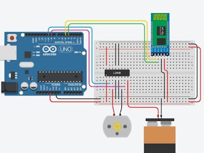
Pwm And Direction Control Of A Dc Motor Via Bluetooth Arduino Project Hub

Sg3525 Pulse Width Modulator Datasheet Pdf Download

L298n Based Dc Motor Pwm Control System Design

Tl494 Pwm Power Amplifier Circuit Faq

Pwm And Direction Control Of A Dc Motor Via Bluetooth Arduino Project Hub

Uc3845 Current Mode Pwm Controller Pinout Feature Datasheet